
Steps Involved in Board Assembly
Printed circuit boards (PCBs) are used to connect various electronic components together. The assembly process consists of several automated and manual steps, which vary from manufacturer to manufacturer, depending on the size and complexity of a particular board.
The first step in the PCB assembly process is adding a copper layer to the substrate, which is the main material that makes up the PCB. The copper layer provides the pathway for electrical current to flow through the entire board, and is also a critical component in ensuring proper connections between all of the individual components on the board.
After the copper layer is added, a protective layer called solder mask is applied to the top and bottom of the substrate, which ensures that the copper will not come into contact with anything other than its intended destination on the board. The next step is to add the solder paste, which will serve as the base for all of the components on the board. This is done by using a screen printer, which applies an even coat of the paste to the areas on the board that will be connected with other parts.
Once the solder paste has been added to the board, the assembler must inspect it for quality. Traditionally, this was done by eye, but for larger batches, it is much more efficient to use an automated inspection machine. Humans tend to get fatigued from looking at such small components for hours, which can lead to inaccurate results. Automated optical inspection machines have cameras that are able to examine the paste and the components on the board from different angles, and can spot issues such as improper thickness, missing components, deviation in component positioning, polarity, and bridging between leads.
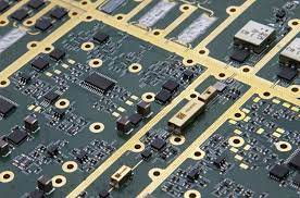
What Are the Steps Involved in Board Assembly?
During this stage, the assembler will also look for through-hole components that need to be added. The assembler can choose between three methods for through-hole part insertion, including manual, wave soldering, and selective soldering. For manual through-hole part insertion, the assembler will place each component on the board and use a soldering tool to solder them into place. The assembler can then clean the board with solvents to remove any excess solder. For the other two methods, liquid flux is applied to the lead ends, and the board is preheated and passed through a solder wave to create the solder joints.
The last step in the assembly process is to check for functionality, which is done by testing each individual component and the overall integrity of the board assembly. Any defects detected at this point can be reworked or discarded, depending on the nature of the defect.
While the aforementioned steps are the main steps involved in PCB assembly, there are other techniques that can be used for more complex boards or to meet certain requirements, such as those found in medical or military devices. Some of these other steps include tab routing, which involves creating V-shaped grooves on both sides of the PCB to define the separation lines for the individual circuit assemblies; and flex routing, which uses a thin film to allow for bending during transport.
