
Flexible PCBs Can Withstand Harsh Environments
When designing PCBs for harsh environments, engineers need to keep in mind that there are a number of factors that can impact the reliability of a board. These include mechanical stress, temperature fluctuations, shock & vibration, chemical & radiation exposure and more. While this may seem like a lot to take into account, fortunately, PCBs can be designed to be robust enough to handle these conditions.
One way to achieve this is by using high-quality materials. This includes selecting a substrate material film that is flexible, tough and incredibly heat resistant, such as polyimide. This is a popular choice for both rigid-flex and flex circuits. It can also withstand many solder reflow cycles and is stable in expansion and contraction when exposed to temperature changes.
Another important factor is ensuring that a flexible pcbs has an adequate bend radius. To do this, engineers need to consider the thickness of the copper traces and how they’re distributed on the board. The thinner the traces, the easier it will be to bend the board. Additionally, engineers should try to minimize the amount of copper on each layer of the flex circuit. This will also help it become more flexible and reduce the chances of damage to conductive paths.
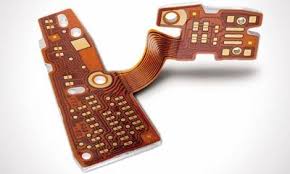
How Flexible PCBs Can Withstand Harsh Environments
It’s also important to use the right fabrication techniques for a flex circuit. For example, etching the substrate in the appropriate manner and using drill-to-copper distance measurements are critical. These methods can help avoid the cracking of traces in areas subjected to repeated stress. Lastly, using pad-only plating (button plating) is beneficial for a flex circuit because it allows fabricators to get higher etch yields and improved flexibility in the conductive path.
Once a PCB has been designed, it’s time to make it a reality. First, engineers will need to add the necessary components and drill holes to the circuit. Next, they will need to route the traces, which involves connecting the segments of each path. This is where it’s crucial to follow the original circuit diagram. Additionally, designers can add labels, identifiers and markings to the traces if needed. This step is vital to ensuring that the final product will be able to withstand harsh environments.
Finally, it’s important for engineers to choose a reliable PCB manufacturer. This means analyzing the manufacturer’s quality control processes, ensuring that they meet industry standards and adhering to their own rigorous manufacturing procedures. Choosing a reputable manufacturer will ensure that the resulting flex circuit is durable and reliable, even when it’s subjected to harsh environments.
In addition, a good manufacturer will have the tools and resources to offer the best value for their customers. This can include options such as adding a protective shielding film to selected areas of the flex circuit, which can help protect against electromagnetic interference. This is especially useful in devices that will be used for medical purposes or in harsh, industrial applications. The EMI shielding is also helpful for protecting sensitive electronics against damage caused by static electricity.
